
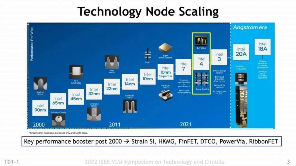
“Intel 4” process-Aiming for Commercialization in 2023 With 7nm, EUV Exposure and 20% Increase in Performance
At this year’s VLSI Symposium in June, Intel alone has 12 papers. Including the short course (technical course), 15 presentations have been made. The highlight is the details of the Intel 4 process. I would like to introduce this content a little more.
For Intel, Intel 4 is a whole new process for Intel after a long time (Photo 01). Both 10nm SuperFin and Intel 7 are processes that are an extension of Intel 10nm (Intel 7 was formerly called 10nm Enhanced SuperFin), and until this generation, ArF + liquid used SAQP (Self-Aligned Quadruple Patterning). I used to draw circuit patterns with immersion Quad Patterning (though I only did SADP twice, so it’s actually 3 times), but Intel 4 will use EUV exposure for the first time.
Here are the general features of Intel 7 (Photo 02). When using the High Performance Library, the density is doubled compared to each other, and the operating frequency can be raised by 20% with the same power consumption. So how specifically did you achieve these? But first, let’s talk about wiring density.
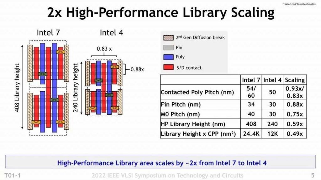
Photo03 is a dimensional comparison between high-performance libraries.
- CPP (Contact Poly Pitch: vertical wiring density in the figure) is 0.83.
- The Fin Pitch (figure horizontal wiring density) is 0.88 times.
It has become Also, although not directly shown in this figure, the wiring pitch of M0 (the wiring layer closest to the transistor) has also been reduced from 40nm to 30nm, and as a result, the width of the library is 0.83 times and the height is 0.59 times. It is said that the area has increased by 0.49 times. In fact, in addition to this
- The gap (dummy gate) between the two transistors has been reduced from 2 fins in Intel 7 to 1 fin in Intel 4.
- The number of fins itself is 3 fins in Intel 4 instead of 4 fins in Intel 7.
There are two changes. By such a matching technique, the area of the CMOS transistor itself could be reduced by half.
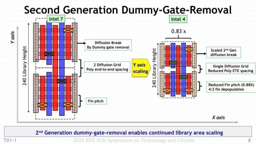
COAG (Contact Over Active Gate) has been adopted by Intel 7 (Photo 04), but there is no particular explanation for the difference between Gen 2 COAG and Gen 1 COAG, so I’m not sure. The material of Contact Gate is different (described later), so it may be Gen 2.
Also, here is the story of deleting the Dummy Gate (Photo 05). By reducing the distance in the Y-axis direction to the minimum, the height can be reduced from 408nm to 240nm. By the way, when it comes to the X-axis direction, the Intel 10nm generation has already adopted Single Diffusion Break, so it looks like Intel 4 has become Single for both the X-axis and Y-axis.
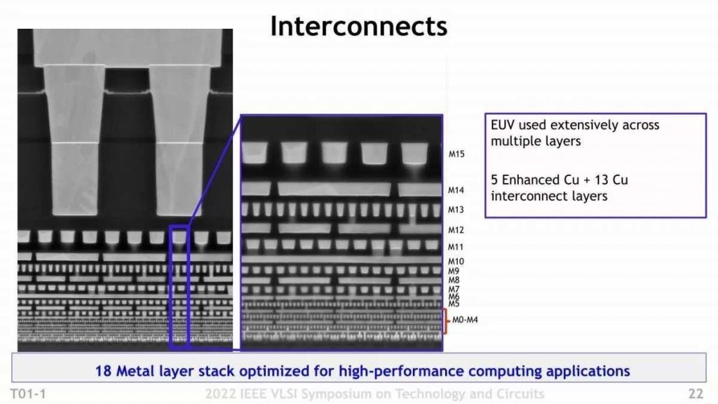
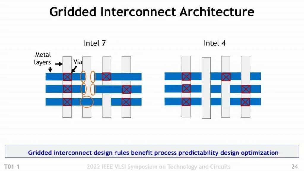
Next, about design rules. Here is a comparison of the Intel 7 and Intel 4 Metal Pitch (Photo 06). On average, it seems that miniaturization is progressing a little, but the bigger thing is the difference in material. Originally, one of the reasons why the Intel 7 or Intel 10nm generations had a difficult time was the electromigration of the wiring layer. In short, it is deterioration of the wiring layer. Electromigration is more likely to occur abruptly when the width of the wiring is shorter than what is called the mean free path of electrons. This value varies depending on the material, but for copper it is about 40 nm, and M0/M1 is far below this (Photo 06 shows the “interval between wires”, not the width of the wires themselves. So with Intel 7’s M0, it’s not 40nm, but at best it’s half 20nm, and M1 is thought to be around 18nm). The reason why cobalt (CO) was used for M0/M1 in the Intel 7th generation is that in the case of cobalt, the mean free path of electrons is about 7.8 nm to 11 nm, which is much shorter than copper, so the Contact Gate or M0/M1 Electromigration is unlikely to occur even when used for such fine wiring. However, cobalt has the problem of much higher resistance than copper (6 times that of copper), which was about to cause wiring delays (or rather, one of the reasons why Intel 7 does not raise the operating frequency so much). I feel like it is). To solve this problem, Intel introduced a new structure called eCu (Enhanced Cu) here. The structure of eCu will be explained later, but this eCu is used for the 5 layers of M0 to M4.
The structure of the eCu is here (Photo 07). In the case of Intel 7, M0 and M1 used cobalt wiring with tantalum (Ta) as the barrier layer, and other wiring used copper wiring with tantalum nitride (TaN) as the barrier layer. On the other hand, in eCu, a cobalt liner layer was constructed on the outside of the copper wiring, and this was covered with a tantalum barrier layer.
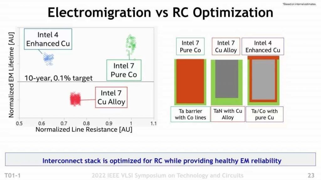
The horizontal line in the center is “the life equivalent to the occurrence of Electromigration with a probability of 0.1% after 10 years”, and by using eCu, the product life of about 10 years can be secured (plus the resistance value is cobalt). Half of the wiring).
In fact, this method is the same as the method proposed by Globalfoundries at IEDM in 2017. Eventually, Globalfoundries stopped migrating to the 7nm generation, so Intel was the first to implement it. Looking at the figure, the eCu structure has a high resistance to electromigration while lowering the resistance value. It is said that Intel 4 says that the operating frequency can be increased by 20% with the same power as Intel 7, but there may be a part that the resistance reduction of this wiring layer also contributes to.
Next is the story of exposure. Although not explicitly stated, it is said that Intel 4 probably uses EUV exposure for M0 to M4 that use this eCu in addition to the transistor layer (Photo 09). Regarding this effect, first of all, the mask can be made sharper, and second, the processing can be completed with one exposure, so the efficiency can be improved 3 to 5 times in terms of the number of processes. However, this is decreasing because it is compared by the number of processes, but in terms of the essential processing time, the throughput is not so high with EUV at the present time. Of course, in the past, it was only one turn to repeat exposure CMP stacking, so it does not mean that the time will not be reduced, but it seems that the time of the exposure itself will be quite long, and if it is subtracted, it may be a slight reduction. I think By the way, here is a comparison of the number of masks and the number of processes (Photo 10), and although the number of masks has decreased, considering that EUV masks are still expensive in terms of cost, how much reduction effect is there? It is unknown if it exists.
However, EUV has another effect, which is that it can draw patterns much more precisely than SAQP. In Photo 05, it was said that the number of Dummy Gates could be reduced by one, but this was possible only with EUV (Photo 11).
By using EUV, it became possible to manage the wiring length precisely, so it became possible to handle it with Single Dummy Gate.
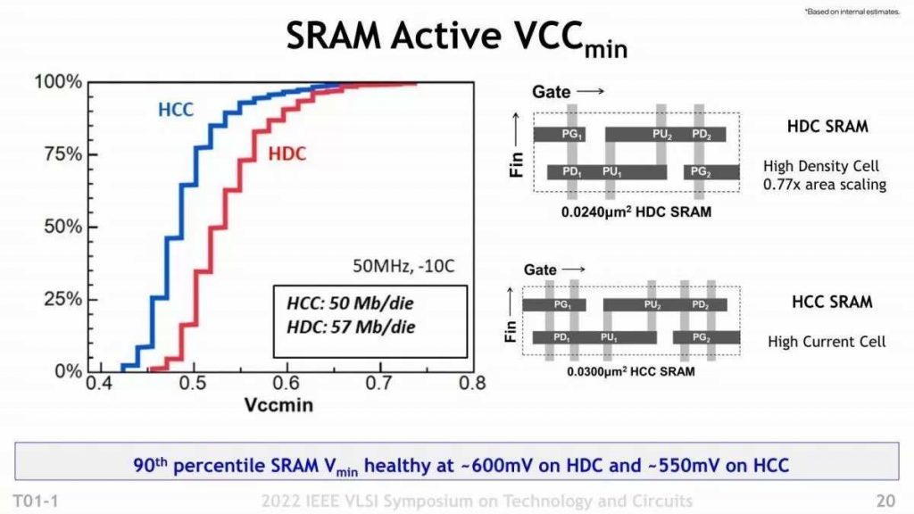
Next, let’s talk about performance. Earlier, it was said that the operating frequency could be increased by 20% with the same power, but the specific result is shown here (Photo 12). In the case of Intel 7, driven by 0.65V, it is possible to improve by 21.5%. By the way, it seems that the upper limit is up to about 1.3V. The operating frequency is not so high (about 3.3GHz even with Intel 7). This is said to be “Industry Standard Core” instead of x86 (specifically unknown), probably using Arm’s Cortex-A76 or its neighborhood. I think it’s because I’m doing it. It is a little interesting that 2 types of options, 6VT (6 types of power supply voltage) and 8VT (8 types of power supply voltage), are offered. As shown on the right, to be precise, 3 to 4 types of voltage can be used for each of the NOTES and the MIMO (NMOS in increments of 190 mV and MIMO in increments of 180 mV), which allows a free balance between performance and power consumption. It is said that it can be adjusted to. Probably 6VT (3 types in short) does not have HVT, and the power consumption can be reduced by the amount that configures the circuit using 3 types of transistors of ULVT/LVT/SVT, but the power consumption increases sharply above 3GHz. On the other hand, 8VT can use HVT in addition to this, and by using this for the critical path, it seems that the increase in power consumption will be a little slower even if it exceeds 3GHz. Regarding SRAM, two types, HDC (high density) and HCC (high speed), are offered, and it is said that HDC can increase the number of SRAM cells by about 25% (Photo 13). Regarding the MIM Capacitor, it is said that it will provide almost double the capacity for the Intel 7th generation, which will contribute to the stable operation of the circuit (Photo 14). Why does it lead to stable operation? Speaking of which, this MIM Capacitor can be used as a decap, which is advantageous for raising the operating frequency.
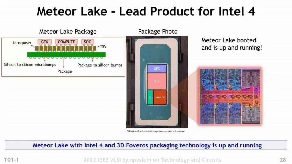
Now, the first product to use this Intel 4 is Meteor Lake. SoC (Chipset) 4 Die configuration, but it is unclear how many of these will use Intel 4 at this time. But at least the compute die and graphics die are definitely Intel 4. The question is, “What’s the situation with that Intel 4 Yield?”. Probably the most frequently asked question is “Meteor Lake with Intel 4 and 3D Foveros packaging technology is up and running.” thing.
At the beginning, Intel said that it published 12 papers this time, 5 of which are related to Intel 4. Specifically, in addition to the T01-1 (Intel 4 CMOS Technology Featuring Advanced FinFET Transistors Optimized for High Density and High Performance Computing) introduced this time,
- C08-1 is an 8-core RISC-V processor with Near Last Level Cache in Intel 4 CMOS.
- C13-3 A 4nm-class CMOS Hybrid Temperature Sensor with 90.9kS/s and 0.7nJ/conversion.
- Intel 4 CMOS C16-1A 7Gbps SCA-Resistant Multiplicative-Masked AES Engine
- C24-1 Intel 4 CMOS Energy-Efficient High Bandwidth 6T SRAM Design
is mentioned. However, all the papers have a similar feeling. For example, C08-1 RISC-V processor + CNC (Compute Near Last Level Cache) is “Intel 4 CMOS test chip boots Linux and performs CNC with RISC-V extension”. In the implementation of the AES engine in C16-1, it is appealing that “If you move, you will get good results,” such as “the Intel 4 prototype demonstrates 1.8x and 50% improvements in area and performance overheads compared to AM AES”. However, I feel very dangerous when I say nothing about Yield.